2020 marked Snap-on’s 100th year, and to mark the occasion, Snap-on released the graphic below:

A symbol appears in both zeros of the one hundred. The first zero has a hexagonal centre to symbolise a socket, this is a link to the origins of the company and the “Game Changer” that is the interchangeable socket. The second zero has the on/off symbol. This shows how Snap-on has adapted to the ever changing landscape of the automotive repair industry and the importance of diagnostic tools to the industry.
The reason we have a 1 and 0 in the On/Off symbol is a link back to the binary system. Interestingly there is a pertinent link between the Binary System, Snap-on Diagnostics, and Cork, Ireland.

Snap-on Diagnostics have an office in Cork. This facility is one of several Snap-on global engineering sites with a proud history of R&D and innovation. The link between Cork and the Binary system dates back further still, in fact all the way back to 1849!
A university professor named George Boole, born in Lincoln England, moved to Cork in 1849, and became the first professor of mathematics in University College Cork. In 1847, Boole introduced his work on Boolean algebra in his first book, The Mathematical Analysis of Logic.
In its most fundamental form, Boolean algebra is based on a mathematical statement being either true or false, on or off, 1 or 0. This logic is fundamental to the operation of modern computing technology.
In recent times, advances in data transfer between electronic control modules on motor vehicles has allowed various systems within the vehicle to communicate at data transfer rates previous impossible.
Boolean logic.
Electronic control modules process data from various sensors and modules controlling multiple systems. Control modules operate on the principle of Boolean logic (the binary system), this is where a statement is either true or false. True is identified by a logic 1, and false by a logic 0. Another set of terms often used are high and low. High relates to logic 1 and low relates to logic 0. High and low is the most suitable terminology because the signal 0 and 1 is actually a voltage applied to an electronic device. One or two inputs (depending on the device) are applied to a component called a logic gate, there is a single output from the gate.
We will look at some simple logic circuits and analyse the inputs/outputs in a truth table. A control module will have in the order of several million such devices within each processor.
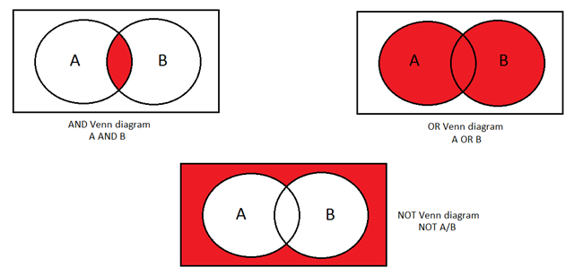
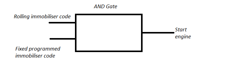
AND diagram.
The common area between A and B indicates an output that is applicable to both A and B.
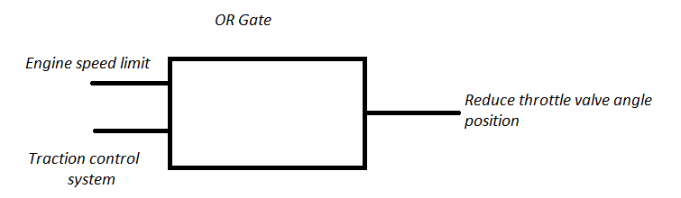
OR diagram.
This relates to an output that is applicable to A or (and) B
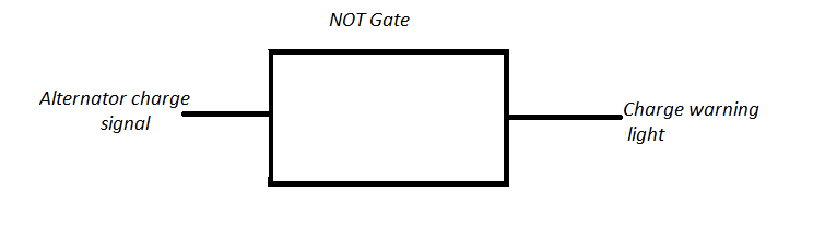
NOT diagram.
This relates to an output that is not applicable to A or B.
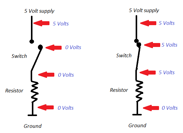
Switched Circuit Theory:
Prior to looking at a transistor operated device, we can use a mechanical switch to get an understanding of the voltage at different points.
Now that we have an understanding of the theory behind logic gates we can analyse an electronic version of each circuit.
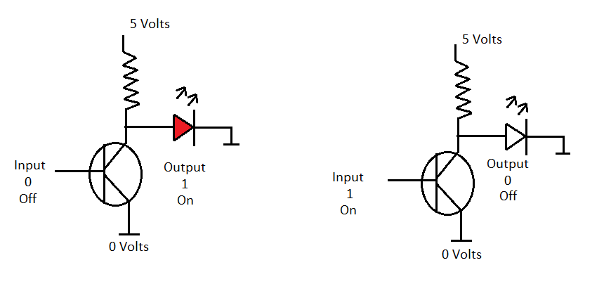
AND Gate.
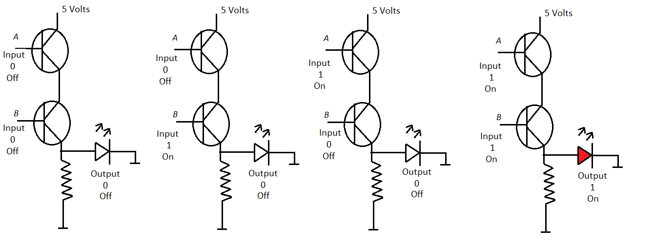
This circuit uses two transistors which are connected in series with one and another, the emitter of the first transistor is directly connected to the collector of the second transistor. A light emitting diode is connected to the output as a visual reference. The emitter of the second transistor is connected to ground via a resistor. The output connection is on the ground side of the second transistor but upstream of the resistor. The applied voltage (5 volts) is connected to the collector of the first transistor. It can be seen from the illustration that even if (only) one of the transistors is switched on, by applying a voltage to the base/emitter circuit, current cannot flow from the supply to ground. It can be seen that there is no voltage applied to the light emitting diode so the LED remains switched off. Only when both transistors are switched on can current flow to ground via both collector/emitter circuits.
OR Gate.
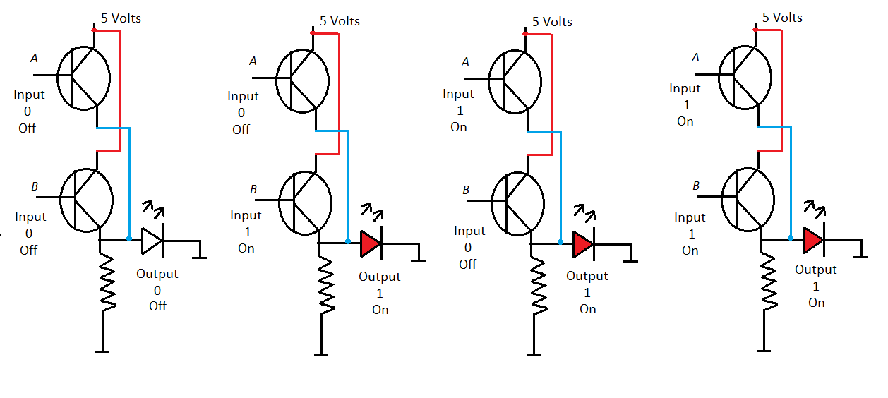
This circuit uses two transistors which are connected in parallel, both collectors have an independent 5 volt supply and both emitters can allow current to flow to ground separately. Again a light emitting diode is used as a visual reference. A voltage is measured at the output point when any one or both transistors are switched on. Again note the output is connected upstream of the resistor.
NOT Gate.
A NOT gate differs from both the AND/OR gates because there is only one input, as with other versions there is only one output. The NOT gate is also referred to as an inverter. This is because the output is the inverse of the input. When a logic 0 is applied to the base of the transistor, the output is logic 1. So when the transistor is switched off, a voltage is available at the output point. The reason this device works is because the resistor is connected between the 5 volt supply and the collector of the transistor. Note, there will be no volt drop across the resistor if current is not flowing within the collector/emitter circuit. When the transistor is switched off there is no path to ground for the current to flow.
A simplified practical example of a AND, OR and NOT Gate is displayed below:
AND Gate.
OR Gate.
NOT Gate.
Example Controller Area Network (CAN) Bus waveform:
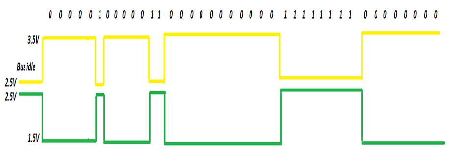
CAN bus uses a different method to assign a numerical value to the bus voltages. A dominant bit, of zero is set, when the CAN High voltage is 3.5 volts and the CAN Low voltage is 1.5 volts. The recessive state, given a value of 1 is when the voltage on both CAN High and CAN Low is 2.5 volts.
The binary system is still fundamental to the operation of the system.
Example Local Interconnect Network (LIN) Bus waveform:
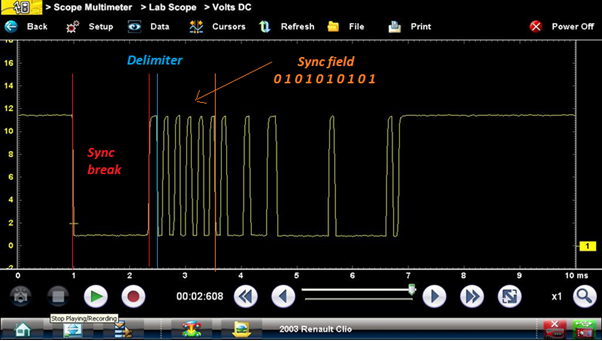
LIN Bus has an idle voltage of approximately battery voltage. During communication the module pulls the Bus voltage towards ground potential, this is a dominant (1) bit. To ensure correct message timing the master LIN node synchronises the other modules on the network with a 10 bit Synchronisation field.
LIN Bus status vs voltage levels: